Thursday, April 23, 2026

RL Filters


An RL filter is a circuit made using a resistor (R) and an inductor (L) to control how different signal frequencies pass through a circuit. These filters are commonly used in signal processing, power electronics, and communication systems.
In the RL Low-Pass Filter, the inductor is connected in series with the input and the resistor is connected to ground. The output is taken across the resistor. At low frequencies, the inductive reactance is small, so the signal passes easily to the output. At high frequencies, the inductor offers higher reactance and blocks the signal, reducing the output. This allows low-frequency signals to pass while attenuating high-frequency components.
In the RL High-Pass Filter, the resistor is placed in series and the inductor is connected to ground. The output is taken across the inductor. At low frequencies, the inductor behaves almost like a short path to ground, so the output is small. At high frequencies, the inductor’s reactance increases, allowing higher-frequency signals to appear at the output.
The cutoff frequency of an RL filter is given by, fc = R / (2πL),
which determines the boundary between the passband and attenuation region.


https://www.facebook.com/photo/?fbid=1386788910131797&set=a.452486110228753


High-frequency noise often interferes with useful signals in electronic circuits. A low-pass filter is designed to solve this problem by allowing low-frequency signals to pass while reducing or blocking high-frequency components.
The simplest low-pass filter is the RC low-pass filter, which uses a resistor (R) in series with the input signal and a capacitor (C) connected to ground. The output is taken across the capacitor.
At low frequencies, the capacitor has high reactance and behaves almost like an open circuit. As a result, most of the input signal appears at the output, so the signal passes through with very little attenuation.
At high frequencies, the capacitor reactance becomes very small. The capacitor provides a low-impedance path to ground, so high-frequency components are diverted away from the output. This effectively reduces high-frequency noise in the signal.
The frequency where the output drops by 3 dB is called the cutoff frequency (fc) and is given by:
fc = 1 / (2πRC)
Above this frequency, the signal decreases at a rate of about −20 dB per decade. Because of this property, low-pass filters are commonly used for noise reduction, signal smoothing, and anti-aliasing in electronic systems.


three main amplifier configurations


A BJT can be used in three main amplifier configurations depending on which terminal is common to both the input and output circuits. These are common-base (CB), common-emitter (CE), and common-collector (CC) configurations.
In the common-base configuration, the base terminal is shared by both the input and output circuits. The input signal is applied to the emitter and the output is taken from the collector. This configuration provides high voltage gain but low current gain, and it is often used in high-frequency applications.
In the common-emitter configuration, the emitter is the common terminal. The input signal is applied to the base and the output is taken from the collector. This is the most widely used BJT amplifier because it provides both high voltage gain and significant current gain, making it useful in many amplification circuits.
In the common-collector configuration, the collector is the common terminal. The input is applied to the base and the output is taken from the emitter. This configuration is also called an emitter follower. It provides high current gain but voltage gain close to 1, making it useful for impedance matching and buffering.
Together, these three configurations allow BJTs to perform different amplification roles in electronic circuits.

Inductance


Current in a coil creates a magnetic field around the wire. When the wire is wound into many turns, the magnetic field from each turn combines and forms a strong magnetic field inside the core. This property of a coil to store energy in a magnetic field is called inductance.
The inductance of a coil depends on several physical factors. The number of turns 👎 increases inductance because more turns strengthen the magnetic field. The cross-sectional area (A) of the core also increases inductance since a larger area allows more magnetic flux to pass through. The core material permeability (μ) determines how easily magnetic flux flows through the core; materials like iron increase inductance significantly. The length of the coil (ℓ) has the opposite effect—longer coils spread the magnetic field, reducing inductance.
These relationships are summarized by the formula
L = μN²A / ℓ, where L is the inductance in henries.
When current flows through the inductor, energy is stored in its magnetic field. The stored energy is given by
W(t) = 0.5Li²(t).
This stored energy is useful in many circuits such as power supplies, filters, DC-DC converters, and switching regulators, where inductors temporarily store and release energy to control current and voltage behavior.


Transistor


A transistor like BC546–BC550 is a small NPN device used to amplify or switch signals. It has three pins: Emitter (E), Base (B), and Collector (C). A small current at the base controls a larger current flowing from collector to emitter.
These transistors look similar but differ in voltage rating and noise performance:
BC546: Handles higher voltage (up to ~65 V)
BC547 / BC550: Medium voltage (~45 V)
BC548 / BC549: Lower voltage (~30 V)
BC549 / BC550 are preferred for low-noise audio circuits
Current gain (hFE) shows how much amplification you get:
A: 110–220 (low gain)
B: 200–450 (medium gain)
C: 450–800 (high gain)
Key limits:
Max current ≈ 100 mA
Max power ≈ 500 mW
Frequency range up to ~300 MHz
In simple terms, use:
BC547/548 for general circuits
BC549/550 for audio (less noise)
Pick A/B/C depending on how much amplification you need


switching using NPN and PNP Transistor


This diagram shows how NPN and PNP transistors are used as switches.
In the NPN (low-side switch), the emitter is connected to ground and the load is placed between Vcc and the collector. When the microcontroller outputs a HIGH signal to the base, the transistor turns ON and allows current to flow from Vcc → load → transistor → ground. This is called current sinking, and it is the most commonly used switching method.
In the PNP (high-side switch), the emitter is connected to Vcc and the load is connected to ground through the collector. When the base is pulled LOW, the transistor turns ON and supplies current from Vcc to the load. This is called current sourcing.
In practice, a base resistor is always required to protect the transistor and microcontroller.

A common emitter amplifier with voltage divider bias


A common emitter amplifier with voltage divider bias is widely used because it provides stable operation and good signal amplification. The two resistors R1 (20 kΩ) and R2 (3.6 kΩ) form a voltage divider that sets the base voltage at about 1.83 V. This ensures the transistor operates in the active region, which is necessary for proper amplification.
The emitter resistor (220 Ω) stabilizes the circuit by reducing the effect of temperature and transistor variations. The capacitor CE bypasses this resistor for AC signals, increasing gain. The collector resistor (1.2 kΩ) converts the amplified current into a voltage output.
When an input signal is applied through capacitor C1, it slightly changes the base current. Due to the transistor’s current gain (β = 100), this small change produces a larger change in collector current (IC ≈ 4.58 mA), resulting in an amplified output at Vout through capacitor C2.
The output signal is inverted compared to the input, which is a key characteristic of common emitter amplifiers. The circuit maintains a stable DC operating point (Q-point), ensuring linear amplification without distortion.


This circuit is a common emitter amplifier using voltage divider bias for stable operation. The resistors (20kΩ and 3.6kΩ) set a fixed base voltage, ensuring consistent biasing despite transistor variations. The input signal enters through capacitor C1, which blocks DC and allows AC to pass. The transistor amplifies the signal, producing a larger inverted output at the collector. The emitter resistor (220Ω) improves thermal stability, while capacitor CE increases gain by bypassing AC signals. Capacitor C2 couples the amplified output to the load.


A common emitter amplifier is one of the most widely used transistor amplifier circuits. It is called “common emitter” because the emitter terminal is shared by both the input and the output circuits.
The input signal Vin is applied to the base of the transistor through the coupling capacitor C1. This capacitor blocks DC and allows only the AC signal to enter the amplifier. The resistors R1 and R2 form a voltage divider that provides a stable bias voltage to the base so the transistor operates in the active region.
When a small input signal is applied at the base, it changes the base current slightly. Because a transistor has current gain (β or hFE), this small change in base current produces a much larger change in collector current. The collector resistor RC converts this current variation into a voltage change at the output.
The output voltage is taken from the collector. A key property of the common emitter amplifier is phase inversion: the output signal is amplified but shifted by 180°. When the input voltage increases, collector current increases, causing a larger voltage drop across RC, which reduces the collector voltage.
The emitter resistor RE improves thermal stability and stabilizes the operating point. Part of this resistor may be bypassed by capacitor C2 so that AC gain remains high while DC stability is maintained. The unbypassed resistor R3 controls the AC gain and linearity.
The total input resistance is determined by R1, R2, and the transistor’s base input resistance. This circuit provides high voltage gain and is commonly used in audio amplifiers, sensor interfaces, and many analog signal conditioning applications.


BJT Gain Boosting Techniques


Driving a load with a very small input current can be challenging. A single BJT helps, but sometimes its gain is not enough. That’s where gain boosting techniques come in.

Basic BJT (NPN)
A BJT uses a small base current to control a larger collector current.
Ic ≈ β × Ib
Typical gain (β) ranges from about 20 to 200. This works well for many applications, but struggles when input current is extremely low.

Darlington Pair (Two BJTs)
Here, the emitter of the first transistor feeds the base of the second. This cascaded setup multiplies the gain:
β_total ≈ β1 × β2
Now, even a tiny input current can produce a large output current. However, the trade-off is a higher base-emitter voltage (around 1.2–1.4 V) and slightly slower response.

Triple Darlington Pair
Adding a third transistor increases gain even further:
β_total ≈ β1 × β2 × β3
This allows extremely weak signals to drive relatively large loads. The downside is even higher voltage drop and increased saturation voltage, which can reduce efficiency.

Each stage amplifies the previous one. More stages → higher gain, but also more voltage drop and slower switching.
Used correctly, these techniques allow precise control of large currents using very small input signals.

Transistor Amplifier (SOA) Safe Operating Area


A transistor amplifier must operate within safe limits to avoid damage, and this is defined by the Safe Operating Area (SOA). The given circuit is a voltage divider biased common-emitter amplifier where R1 and R2 set a stable base voltage, Re provides thermal stability, and Rc converts collector current into output voltage, while C1 and C2 allow AC signals to pass and block DC. On the graph, the DC load line shows all possible operating points without input signal, and the Q-point represents the steady operating condition. When an AC signal is applied, the operation follows the AC load line, allowing the signal to swing around the Q-point. The shaded region represents the SOA, which defines the safe limits of collector current, collector-emitter voltage, and power dissipation. If the transistor operates outside this region, it can overheat, break down, or fail due to excessive power. To ensure proper operation, the Q-point is set near the center of the load line, enabling maximum symmetrical signal swing without distortion while staying within safe limits. Proper selection of Rc, Re, and load resistance ensures stable biasing, efficient amplification, and reliable operation of the transistor.

BJT Amplifier Biasing


This circuit shows a BJT amplifier with voltage divider biasing, designed to keep the transistor stable.
The resistors RB1 and RB2 create a fixed base voltage VB. This sets the base current IB, which controls the collector current IC. Because of this divider, the circuit becomes less sensitive to transistor variations, giving better stability.
The emitter resistor RE plays a key role in stability. If current increases, voltage across RE increases, which reduces base-emitter voltage and brings the current back down. This is called negative feedback.
Capacitors have specific purposes:
C1 allows AC signal to enter while blocking DC
C2 passes amplified output signal
CE bypasses RE for AC, increasing gain
The load resistor RL converts collector current changes into output voltage.
The graph below shows the load line and Q-point (operating point). The Q-point is set near the middle of the load line so the signal can swing properly without distortion.
Overall, this biasing method is widely used because it provides good stability, predictable operation, and reliable amplification.

Voltage Divider BJT Amplifier


This voltage divider BJT amplifier provides stable and reliable amplification by using a proper biasing method. The resistors R1 and R2 form a voltage divider that sets a constant base voltage, ensuring the transistor operates in the active region even if temperature or transistor gain changes. The input signal is applied through capacitor C1, which blocks DC and allows only the AC signal to pass into the base.
The emitter resistor Re adds thermal stability by controlling the emitter current, preventing the transistor from drifting out of its operating point. For AC signals, capacitor C2 bypasses part of the emitter resistance, which increases the overall gain while still keeping DC stability. On the collector side, resistor Rc converts variations in collector current into voltage changes, producing the amplified output signal.
Overall, this circuit offers a good balance between stability and gain, making it one of the most commonly used BJT amplifier configurations in practical electronics.

Darlington Switch


A Darlington switch uses two NPN transistors connected in a way that greatly increases current gain. When the switch is pressed, a small input current flows through resistor RB into the base of the first transistor (TR1). This current is amplified and passed to the base of the second transistor (TR2). As a result, TR2 conducts a much larger collector current, allowing the load RL to draw significant current from the supply.
Because the total current gain is approximately the product of both transistor gains (β1 × β2), even a very small input current can control a large load. This makes the Darlington pair useful when weak signals need to drive high-power devices like relays, motors, or lamps.
When the switch is OFF, no base current flows, so both transistors remain OFF and the load is disconnected. When the switch is ON, both transistors saturate, effectively acting like a closed switch and allowing current through the load.
One important point is that the Darlington pair has a higher base-emitter voltage (about 1.2–1.4 V) compared to a single transistor. This should be considered in low-voltage designs. Despite this, it remains a simple and effective way to achieve high current amplification.

NPN Transistor Operation


A transistor isn’t controlling voltage directly—it’s controlling current. An NPN transistor uses a small base current to control a much larger current flowing from collector to emitter. When about 0.7 V is applied between base and emitter, it turns ON and current starts flowing. No base current means it stays OFF, just like an open switch.
There are three working modes. Cut-off: no base current, so no output current. Active: output current follows the base input—this is where amplification happens. Saturation: fully ON, acting like a closed switch with maximum current.
The graph shows how collector current changes with voltage for different base currents. More base current shifts the curve higher, meaning more output current. This is why transistors are used everywhere—from switching circuits to signal amplification.

RF Connector Types


Choosing the right RF connector isn’t just about fit—it directly affects signal quality, frequency performance, and reliability. This chart organizes connectors by size and frequency range, making selection easier.
At the smallest end, ultra-miniature and microminiature types like MMCX, MCX, and SMP are used in compact devices such as mobile antennas, routers, and high-density systems. They support up to around 6–40 GHz depending on the type, but are mainly chosen for space-saving designs.
Miniature and subminiature connectors like SMA and SMB are extremely common. SMA, for example, goes up to about 26.5 GHz and is widely used in RF testing, communication systems, and lab setups due to its balance of size and performance.
Moving to medium connectors, BNC and TNC are easier to handle and commonly used in test equipment, video signals, and rugged environments. Their frequency range is lower, but they offer strong mechanical connections.
At the larger end, connectors like Type N and DIN 7/16 are built for high power and outdoor telecom applications such as base stations. They handle lower frequencies but provide excellent durability and low signal loss.
In short, smaller connectors = higher frequency and compact use, while larger connectors = higher power and rugged applications.

Tuesday, November 25, 2025

Alto TS315 2000 watts


TS315

2000-WATT 15-INCH 2-WAY POWERED LOUDSPEAKER
  • 2000 W peak (1300 LF + 700 HF) 1000 W continuous RMS (650 LF + 350 HF)
  • 15-inch (381 mm) LF driver, 3-inch (76 mm) high-temperature voice coil
  • 1.4-inch (35 mm) neodymium magnet HF driver with precision wave guide
  • Pole-mountable, wedge monitor, bracket installation or flown application with integral M10 suspension points
  • Integrated 2-channel mixer with dual XLR 1/4-inch combo mic/line inputs, independent level controls, XLR Link output, Contour EQ switch and Ground-Lift switch
  • Custom-engineered high-efficiency class D amplifiers with passive cooling design – no fan means the speaker runs cleaner, quieter and has greater long-term reliability
  • Designed and tuned in the USA 

Expectations Exceeded.

The new Alto Professional Truesonic TS3 Series does everything you demand in a no-compromise family of professional loudspeakers. These speakers solve every performance and installation challenge you have. They are high-performance in every sense: Their new transducers and amplifiers enable them to play extremely loud and clear, without compromise or restriction. And they are “high-performance” from a concept and manufacturing standpoint—we made sure that every aspect of their design outperformed what it had to do. The end result are loudspeakers that achieve a level of excellence and refinement that defies expectations. Defies your expectations.

There are four models in the new TS3 range: The TS308, TS310, TS312 and TS315, with 8-10-12- and 15-inch woofers respectively.  The range shares a new 2000-watt peak (1000-watt continuous) amplifier, a significant advance over the 1100-watt peak (550-watt continuous) amplifiers in the TS2.

The four models boast all-new low-frequency drivers, designed to play louder and handle more power than their already-impressive predecessors, the wildly-successful TS2 Series. They also have a new horn-loaded high-frequency driver. This impressive transducer has a brand-new heat sink design that provides exceptional heat dissipation for impressive power-handling, even at all-night-long concert levels. Because these new drivers can safely handle the additional power, the TS3’s take full advantage of the increased wattage and will play at higher SPLs with lower distortion.

We’ve even made the TS3’s easier to use, with an updated control panel and clearer control indications and detents that make for a faster, more precise setup.

2000 watts of bi-amplified power, newly-designed drivers and easier, more satisfying controls and setup—the new TS3 range doesn’t merely meet your requirements. It makes you re-think what’s possible.


TECH INFORMATION

  • Output Power: 2000 W peak (1300 LF + 700 HF) 1000 W continuous RMS (650 LF + 350 HF)
  • LF Driver: 15-inch (381 mm) LF driver, 3-inch (76 mm) high-temperature voice coil
  • HF Driver: 1.4-inch (35 mm) neodymium magnet HF driver with precision wave guide
  • Crossover: 2 kHz
  • Maximum SPL: 134 dB peak, 131 dB continuous (dB SPL @ 1 m)
  • Frequency Response: 50 - 20 kHz (+/- 3 dB)
  • Frequency Range: 43 Hz - 22 kHz (-10 dB)
  • Horn Coverage: 90° H x 60° V nominal
  • Equalization: Contour Switch Low and High Frequency +3dB Boost
  • Connectors: (2) XLR/TRS 1/4” (6.35 mm) combo inputs, (1) XLR link output, (1) IEC power cable input
  • Controls: (2) Volume, Power on/off switch, Contour switch, Ground-Lift switch
  • Indicators: 2 x Power LED (front and rear), Clip limiter LED
  • Protection: Electronic clip, Thermal and transducer overdrive protection
  • Power Connection: IEC with Mains Fuse
  • AC Voltage Input: 100,110-120,220–240 V, 50/60 Hz
  • Enclosure: Trapezoidal, injection-molded, polypropylene enclosure, with perforated steel grille
  • Mounting/Installation: 36 mm standard pole mount, Wall or ceiling mount using TSB125 bracket, Flown application with integral M10 suspension points, Wedge monitor
  • Dimensions: (H x W x D): 25.7” x 16.6” x 15.4” / 652mm x 421mm x 392mm
  • Net Weight: 41.3 lbs. / 18.8 kg.
  • Design Origin: Designed and tuned in the USA
  • Accessories: TSB125 Bracket, TS215 Cover


Wednesday, August 20, 2025

Fall 2025 - SSE Class Tentative Schedule

 Fall 2025 - SSE Class Tentative Schedule 

  • One Sharing - Center Level Sharing - After Eshwaramma  Day
  • Class level sharing  (Feb)


Topic 1 - Swami Life

Monday, August 11, 2025

Sai Unity Center Audio /Video Systems

 Sai Unity Center Audio /Video Systems

Description

The Boston Unity Center (SCU) Audio System consists of the following components:

1.       3 pairs of speakers

a.       2 forward stand power speakers (each on both sides of the alter)

b.      2 floor monitoring passive speakers (each on the floor by singers and musicians)

c.       2 side passive speakers (each on both sides of the hall)

2.       A Markie Master Console Mixer

3.       2 Peavey Power Amplifiers

4.       1 Snake from Master Console to singers and musicians


How to Power ON Audio System

Here is the standard operating procedure to power on SCU Audio System.


1.       Connect Sennheiser microphones to color coded wires from snake for ladies, men and musical instruments. Setup microphones on each mic stand.     

a.       Ladies:   1- Red, 2- White, 3 -Blue

b.      Men: 5- Orange, 6 -Yellow, 7 - Gray

c.       Tabla: 8 - Green

d.      Harmonium 9 - Green

2.       Turn power switch ON for the yellow Power Surge Protector (on the floor by the table)

3.       Turn power switch ON for the Markie Master Console Mixer (switch at the front right-hand side)  

a.       Mute ALL Channels

4.       Turn power switch ON Both Peavey amplifiers

5.       Turn power switch ON both forward stand power speakers


How to Power OFF Audio System

To power OFF the SCU Audio System, follow the procedures below:


  1. Mute ALL channels on Markie Master Console Mixer
  2. Turn power switch OFF both forward stand speakers (note these are power speakers)
  3. Turn power switch OFF Both Peavey amplifiers
  4. Turn power switch OFF on the Markie Master Console Mixer
  5. Turn power switch OFF on the yellow Power Surge Protector (on the floor by the table)
  6. Disconnect ALL Sennheiser microphones and return it to their respective case


Note:

1.       Before you turn on the zoom laptop make sure the audio system is turn on so that it will automatically sense the Makie Mixer and load the correct driver for zoom audio.

2.       DO NOT plug in any musical instruments such as keyboards, guitars etc directly into the Markie Master Console.  Please consult your Audio Team for an DI adaptor.

Tuesday, July 15, 2025

Tone Stack - Fender

 Tone Stack 


How The Guitar Amp Tone Stack Work

Tone stack is important part of guitar amp , which directly sculpts the tone of guitar amp.If you want to play guitar better, it is important to know deeply about tone stack, how does it work and how to adjust it.
Magnetic guitar pickup model turns out to be a second-order, low-pass filter and has a strong low middle emphasis and little high frequency response - overall a very muddy and muffled sound. So they need compensate by amp.
To hear the natural sound of a pickup, use a typical guitar amp with the middle set to full, and bass and treble on 0. This is actually sets a flat response in the amp. That's the whole point of these tone controls providing compensation for the natural sound of a pickup - the middle control simply boosts the pickup's normal'middley' sound. The treble and bass controls do the opposite - they boost higher and lower frequency levels, leaving a notch in-between for middle cut.
The Fender/Marshall/VOX TMB(Treble Mid Bass) tone stack has been around since the 1950's and has become a staple with Fender and Marshall amps.This design of tone stack is still used in the modern amps.
The TMB stack is made up of several low and high pass audio filters that work together to their magic. It's a relatively low impedance circuit (high load) so it works best when fed by a low impedance source such as a cathode follower like in the 5F6A, JTM45 and many other amps. So, in many amp, tone stack commonly connects behind one cathode follower.
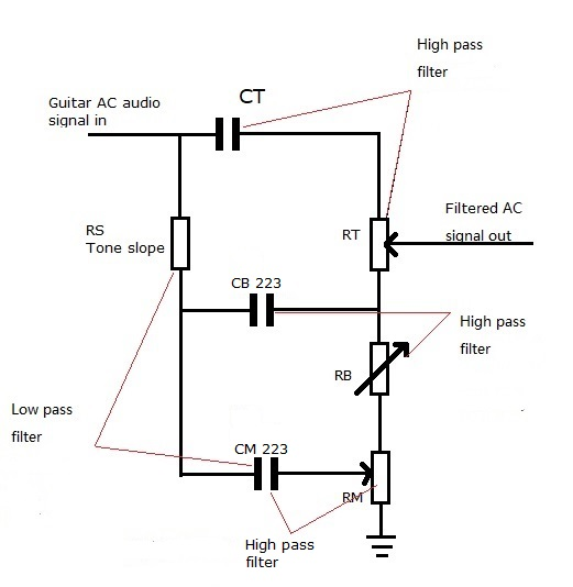
The input splits part traveling through the "treble capacitor" and the rest passing through a resistor to a network of capacitors and pots making up the bass and midrange controls ( midrange pots are optional and are often replaced with a resistor)Everything joins back at the treble pot, which is, in a way, a mixer between the filtered treble (all the lows removed by the low value capacitor) and the bass and midrange circuit.

Audio filter reviews
Before we discuss the tone stack circuit which is surprisingly complex due to the interactive nature of its four audio filters, we simple overview simple RC (resistance-capacitance) filter circuits.First, we know: Capacitor can block direct current and let alter current passing through, sodifferent combinations of capacitor and resistor can be comprised of different type filters.
Low pass filter has a resistor first followed by a capacitor connected to ground.It allows low frequencies to pass but high frequencies are blocked.
The cutoff freq of low pass filt is below :
f(cutoff)=1/(2*3.14*R*C)
R---Ohm,C---Farads
Example:
Bass pass filter of TMB of 5F6A is by Rs and CM.Rs is 56k, CM 0.022uf(223). Then the cutoff freq of low pass filter of Rs and CM is 129hz.


High pass filter has the capacitor first followed by a resistor connected to ground. A high pass filter allows high frequencies to pass but blocks low frequencies.


Tone stack overview


Tone stacks of three brand guitar amp
RS
CT
RT
CM
RM
CB
RB
VOX
100k
56p
B250K
223
B20K
223
A1M
Marshall
33K
470p
B250K
223
B20K
223
A1M
Fender
56K
270p
B250K
223
B20K
223
A1M

Tone stack is by one low pass and three high pass filters. The Tone Slope Resistor RS is important part in tone stack,it takes two important roles in tone stack.
Frequency divider:
RS works as a frequency divider with CT(Treble Cap).The high frequencies signal pass around CT and low and mid frequencies passing through RS to the CB (Bass Cap)and CM (Mid Caps).

A larger value Tone Stack resistor will pass fewer bass and mid frequencies so its value changes the balance or "slope" of the tone stack's frequency response.
The treble high pass filter made up of the CT(Treble Cap)+ RT(Treble Pot) blocks frequencies below approximately 2359Hz to 2184HZ(Fender), allow higher frequencies to pass.The high frequencies are sent to the top terminal of the RT. The bass and mid frequencies signals that pass through the bass and mid filters flow to the RT's lower terminal so the RT is a balance control that allows you to select between the high and low frequencies at its outside terminals.
Low pass filter:
RS + CM (Mid Cap )form the only low pass filter of tone stack filtering high frequency signal and work with two high pass filters (CB+RB,CM+RM). These circuits constitute two band pass filters removing frequencies above and below the desired band of frequencies.The freq range of these band filters are controlled by RB(Bass control)and RM(Mid control). The cutoff freqs of low pass filter in different amps below:

 
RS+CM low pass filter cutoff freq
VOX
72HZ
Marshall
219HZ
Fender
129HZ
One end of CM is connected with RM, this is difference with general low pass filter that the capacitor is connected with ground.The mid & high freq signals from band filters go to one end of the RT through RM, mixing with high freq signal from high pass filter.
The cutoff frequency of high pass filter controlled by RB varies between 7.2Hz and 361Hz. With the RB full up the bass high pass filter only blocks frequencies below 7.2Hz so all guitar and bass frequencies get through. With the RB full down the filter blocks frequencies below 361Hz so most of the bass is filtered out.
The cutoff frequency of high pass filter controlled by RM varies between 361Hz to infinitely high. With the RM full up the mid high pass filter only blocks frequencies below 361Hz.With the RM full down the mid filter blocks all frequencies.
Freq flow in tone stack below.


RM works in tone stack


The combination of the low pass filter which formed by RS+CM and high pass filters which formed by CM+ RM creates a band pass filter. So only mid freqs signals pass through.
The RM control this band pass filter that functions like a mid frequency volume control. At higher RM, this band filter acts as a simple high pass filter which blocks low freq signals but allows mid freq signals through. As RM is turn down , the mid filter's cutoff frequency increases.The cutoff frequency runs from 361Hz with the RM max, to infinitely high with the RM zero.
A high pass filter with an infinitely high cutoff frequency blocks all frequencies so no audio will pass.
The RM below the wiper comes after the low pass filter, which let some mid and high freq signals pass through the filter. Only turning the RM to zero, the RS + CM low pass filter could cut off all frequencies above cutoff, let bass freq signals pass to the RT.

RB works in tone stack


RS+ CM form low pass filter, The bass and mid freq signals pass on to the CB. CB + (RB+ RM) form high pass filter, the RB blocks low frequencies.
By filtering the guitar audio through a low pass filter followed by a high pass filter (Bass control) a variable band pass filter is created that only affects bass freq signals.
With the bass high pass filter's resistance of RB1M + RM 20K = 1.020M with the RB max gives a cutoff frequency of 7.2Hz. With the bass high pass filter's resistance of 0 RB +RM 20K = 20K with the RB minimum gives a cutoff frequency of 361Hz. Note the mid filter's lowest cutoff frequency is 361Hz so the bass and mid filters match up perfectly.
The RM below the wiper comes after the low pass filter let some mid and high freq signals pass through the filter to the CB. The RB has no effect when the RM and RT are full down

RT works in tone stack


CT + (RT+ RM ) form high pass filter, the high freq signals pass across the top of the tone stack.RS +CM form low pass filter, the bass and mid freq signal flow through the RS and CB around to the RT.
Turning the RT does not change the CT+ RT high pass filter cutoff frequency because the RT full 250k of resistance is always in the filter's path to ground--moving the RT wiper does not change this.Turning the RT adjusts the balance between high frequencies on the top side of the RT and Bass & Mid frequencies on the bottom side of the pot.
The RM is added to the treble high pass filter's resistance. The treble high pass filter's resistance ranges from RT with the RM set to minimum to RT+RM with the RM set to Max.The CT + RT high pass filter blocks frequencies below:

 
Cutoff freq of( CT+RT+RM)RM max
Cutoff freq of (CT+RT+RM)RM min
VOX
10531(HZ)
11373(HZ)
Marshall
1355(HZ)
1254(HZ)
Fender
2184(HZ)
2359(HZ)

The RB setting has no effect on the treble high pass filter cutoff frequency because the treble filter's path to ground can flow through the CB and CM to flow around the Bass Pot.
The RS got its name because its resistance affects the balance between high frequencies that flow across the top of the tone stack and bass & mid frequencies that flow below through the rest of the tone stack. A smaller RS will tilt the frequency balance toward bass frequencies by reducing treble and increasing bass. A larger resistor will tilt it toward high freqs and less bass. A larger RS will also reduce the Tone Stack's load (raise its impedance). That's one of the reasons the Fender blackface amps use a 100k Tone Slope resistor.

Conclusion

 
Low-Freq response(HZ)
High-Freq response(HZ)
VOX
30
11373
Marshall
68
1355
Fender
47
2359
With the bass and treble controls at minimum, the midrange control determines the overall attenuation for all guitar frequencies. When the bass control setting is increased, it allows bass to bleed back into the mix, reducing the attenuation for its passband.
The Marshall midrange control offers more midrange at the top end of the control setting, but a more accelerated gain variation depending on the setting. The 5F6-A, on the other hand, has less maximum midrange, but finer midrange control.

RL Filters

  An RL filter is a circuit made using a resistor (R) and an inductor (L) to control how different signal frequencies pass through a circuit...